3-Bit DAC Breadboard Circuit
Analog Discovery 3 Op-Amp (TL072) MOSFETs LTSpice Simulation Breadboarding

Summary

Project Overview

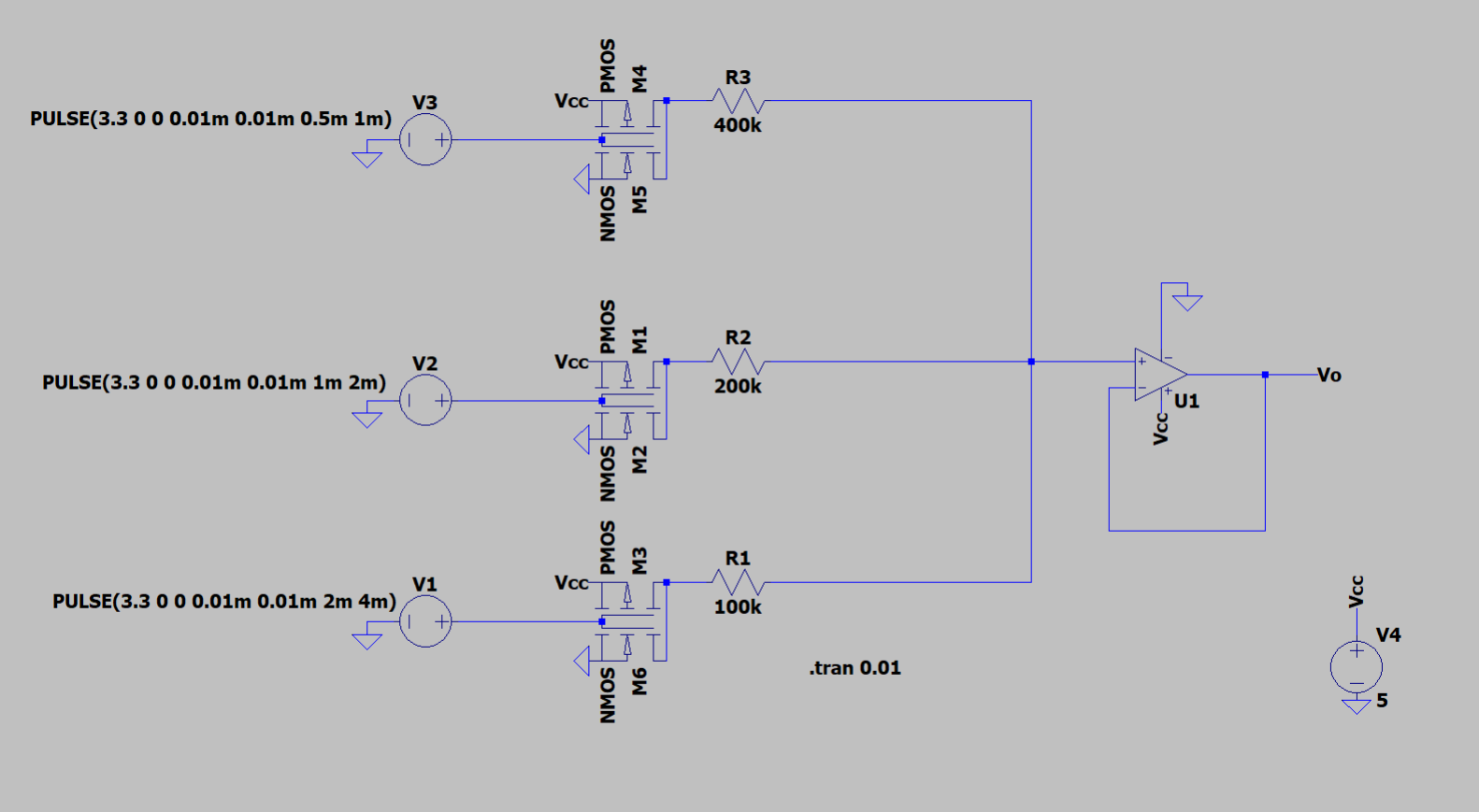
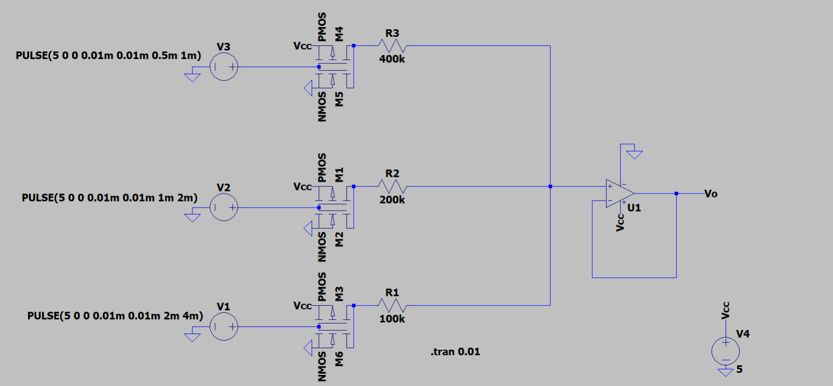
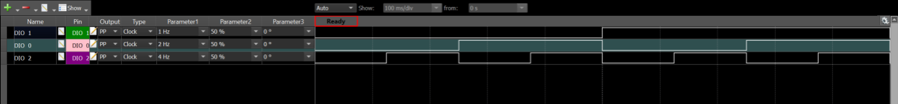
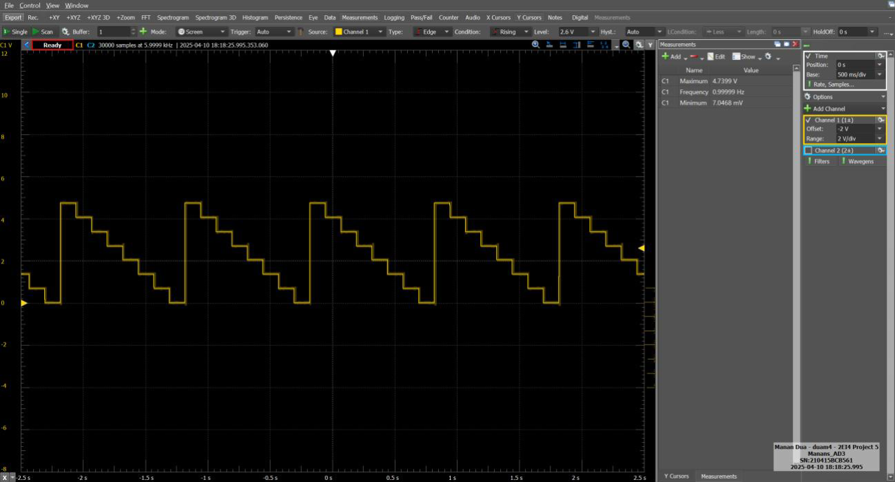
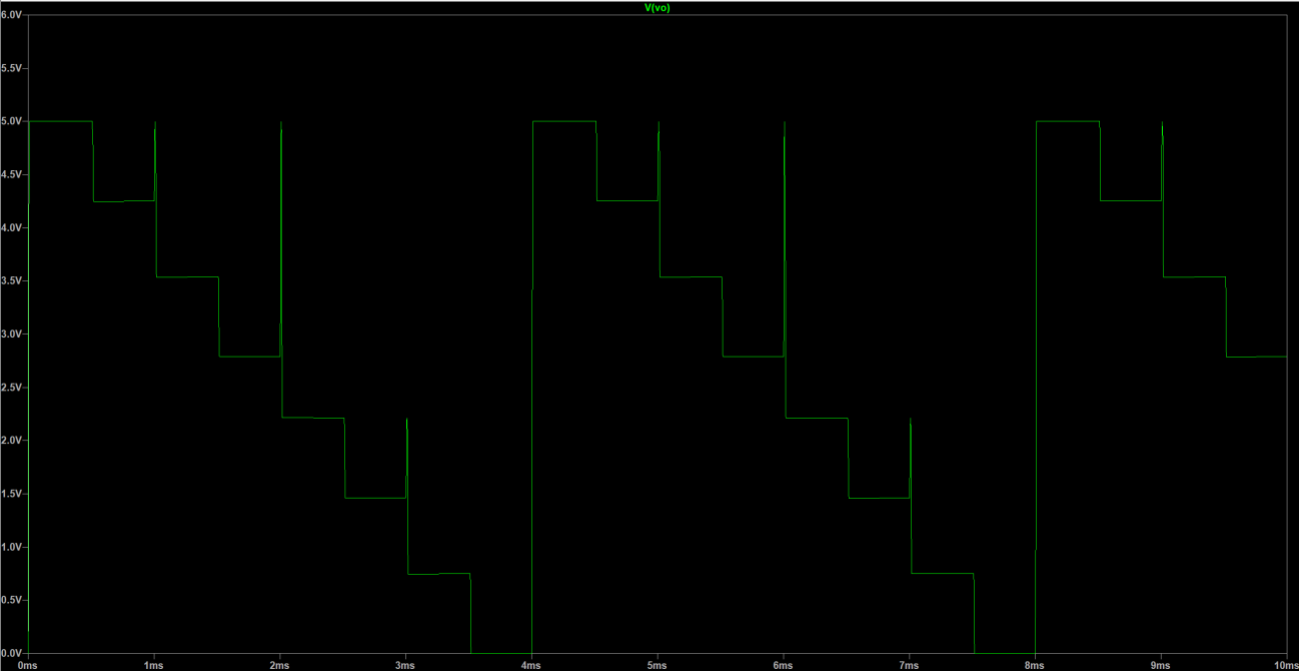
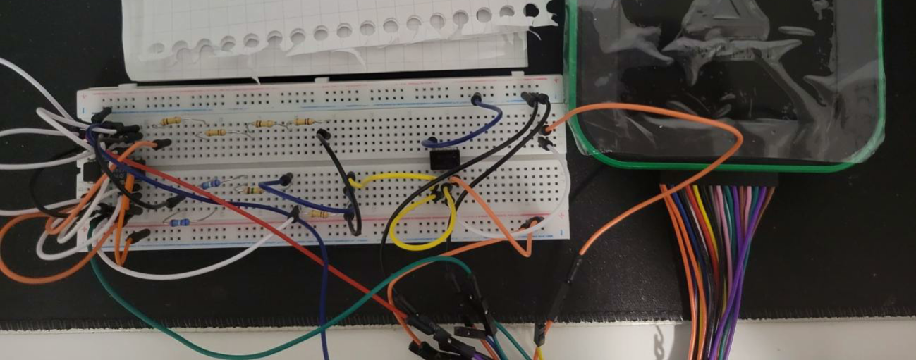
The goal of Project 5 was to design, simulate, and build a 3-bit Digital-to-Analog Converter (DAC) with a full-scale output of 5 V. Three digital input bits feed a weighted resistor network, and the resulting analog voltage is buffered by a unity-gain op-amp stage.

Each bit’s weight is set by R_REF = 100 kΩ:

  • R1 = 100 kΩ (LSB)
  • R2 = 200 kΩ
  • R3 = 400 kΩ

MOSFET switches ensure input lines draw < 1 µA. The final circuit produces an output voltage proportional to the binary input, buffered to prevent loading.

Weighted-Resistor DAC Schematic (Figure 1)

Design

Circuit Topology

The DAC core is a binary-weighted resistor network. Each digital input (V1, V2, V3) drives both a P-MOS and an N-MOS transistor to connect either +5 V or 0 V into the resistor ladder without drawing input current. Because of the complementary MOS topology, logic is inverted:

  • 5 V = logic 0
  • 0 V = logic 1
Simulation Schematic

Component Details

The weighted resistors are:

  • R1 = 100 kΩ (LSB)
  • R2 = 200 kΩ (constructed from 150 kΩ + 2×24.9 kΩ in series)
  • R3 = 400 kΩ (4×100 kΩ in series)

The resistor node drives a non-inverting unity-gain buffer (op-amp) to isolate and maintain the voltage. This buffer draws negligible current, preserving the weighted sum accuracy.

References:

  • W. Storr, “Binary Weighted Digital to Analogue Converter,” Basic Electronics Tutorials.
  • Simply Put, “Making a DAC Using a Resistor Ladder,” YouTube.

Measurement & Analysis

Digital Input Setup

The AD3’s pattern generator drove the three GPIO pins (3.3 V levels) as digital inputs, cycling through all 3-bit codes. Although the DAC was designed for 5 V logic, 3.3 V inputs still switch the MOSFET gates reliably. Op-amp supplies were +5 V / −5 V, and the oscilloscope measured the buffered output.

Digital Input Configuration (Figure 3)

Oscilloscope Output

The scope captured the DAC output as the input code increments from 000 to 111. Each step ideally changes by 5 V / 7 ≈ 0.714 V. The measured waveform shows distinct voltage levels corresponding to each code.

Oscilloscope Output (Figure 4)

Gain Error

Gain error is the deviation between expected and measured full-scale voltage. The ideal full-scale is 5 V, but the measured peak is ~4.74 V. Unity-gain buffer gain error:

Error = (V_Expected − V_Actual) / V_Expected 
      = (5 V − 4.74 V) / 5 V 
      = 5.2 %

Maximum Differential Non-Linearity (MDNL)

MDNL quantifies the largest deviation between ideal and actual step size. For 3 bits, ideal step = 5 V / 7 ≈ 0.714 V. Measured step ≈ 0.697 V. Thus:

V_ideal = 5 V / (2³ − 1) = 0.714 V 
V_actual = 0.697 V 

MDNL = |V_ideal − V_actual| / V_ideal 
     = |0.714 V − 0.697 V| / 0.714 V 
     ≈ 2.42 %

Offset Error

Offset error is the output when input code = 000 (should be 0 V). Measured ~7.05 mV. Causes include MOSFET threshold mismatches and op-amp offset. Thus:

Offset Error = 7.05 mV
Simulated Output with 5 V Input (Figure 5)

Discussion

Origins of Errors

Deviations arise from:

  • 3.3 V input limitation (AD3 GPIO) instead of 5 V specification—MOSFET gates partially on.
  • Resistor tolerances (±1%–±5%) in R_REF network.
  • Op-amp offset and finite open-loop gain causing slight gain error.
  • Wiring and breadboard parasitics introducing noise.

Alternate Designs

Two common 3-bit DAC topologies:

  • Binary-Weighted Resistor Network: Simple resistor values proportional to bit weight. Easy to calculate for 3 bits but requires precise high-value resistors (100 kΩ, 200 kΩ, 400 kΩ).
  • R-2R Ladder Network: Uses only two resistor values (R, 2R), improving matching and reducing tolerance sensitivity. Preferred for higher-bit DACs; slightly more complex routing on breadboard.

For this 3-bit design, binary-weighted was chosen for simplicity and minimal component count, despite R-2R’s potential accuracy advantages.

References

  1. W. Storr, “Binary Weighted Digital to Analogue Converter,” Basic Electronics Tutorials, Jun. 10, 2022. View Source
  2. Simply Put, “Making a DAC Using a Resistor Ladder Op-Amp Weighted Summing Amplifier,” YouTube, May 4, 2020. View Video