DC Power Supply Output Waveform
Analog Discovery 3 Full-Wave Rectifier RC Filter LTSpice Simulation Breadboarding

Summary

Project Overview

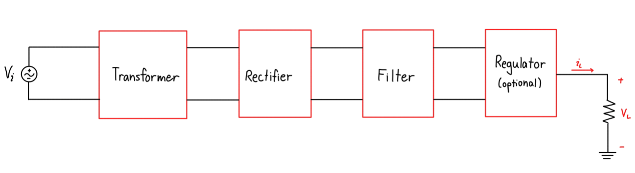
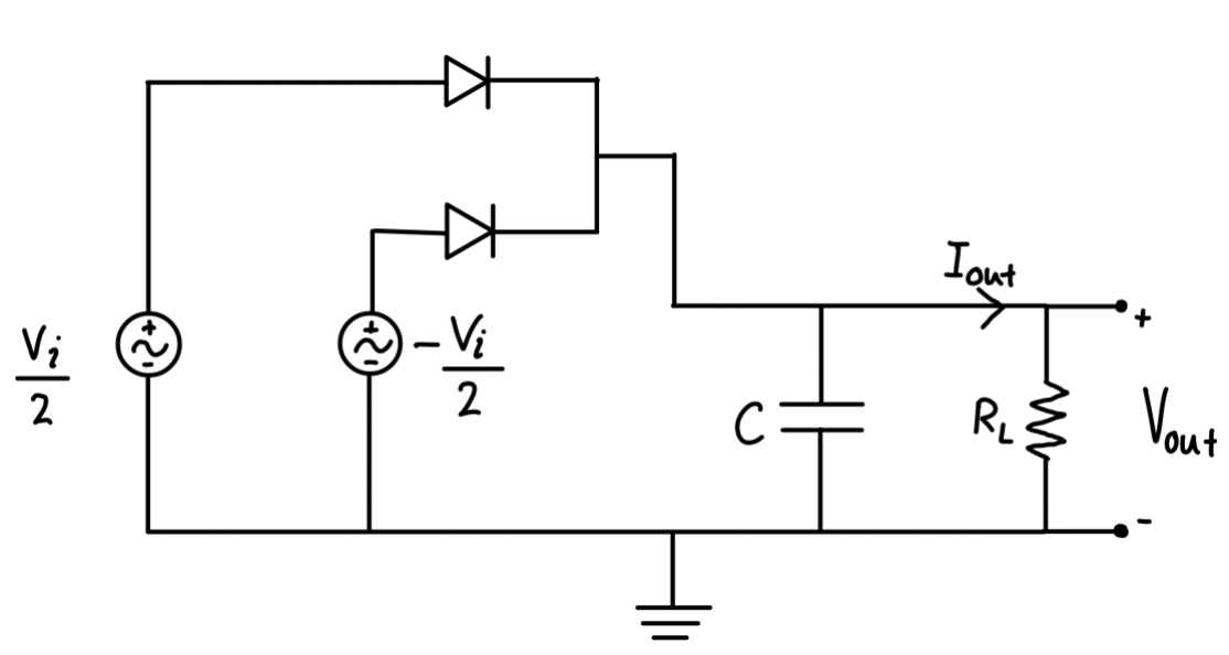
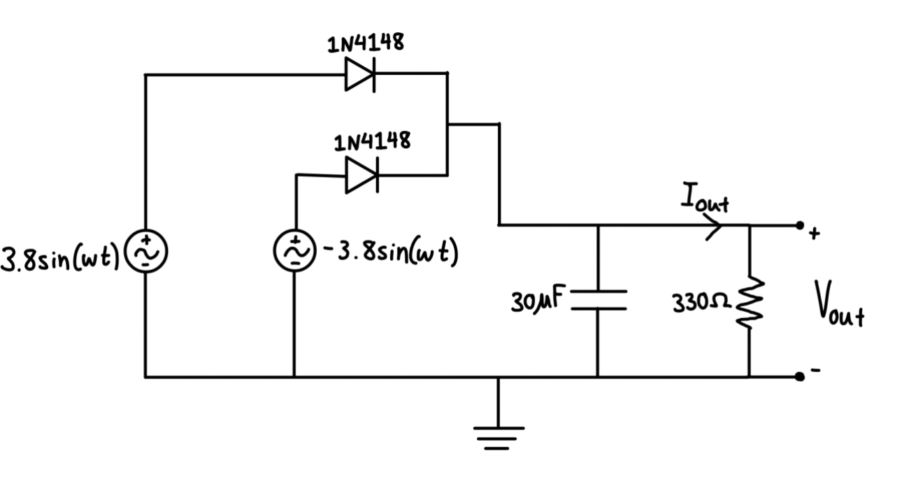
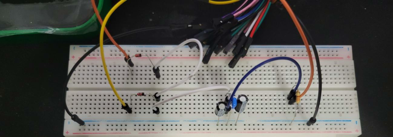
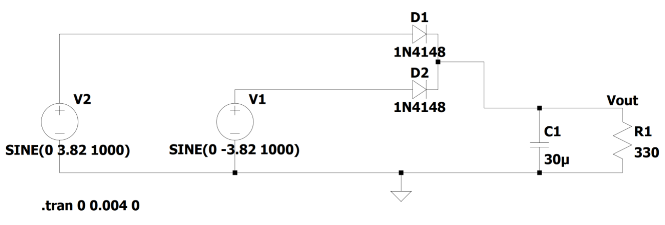
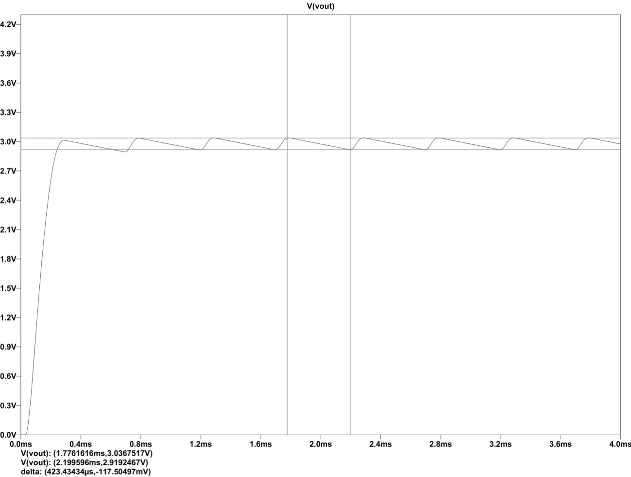
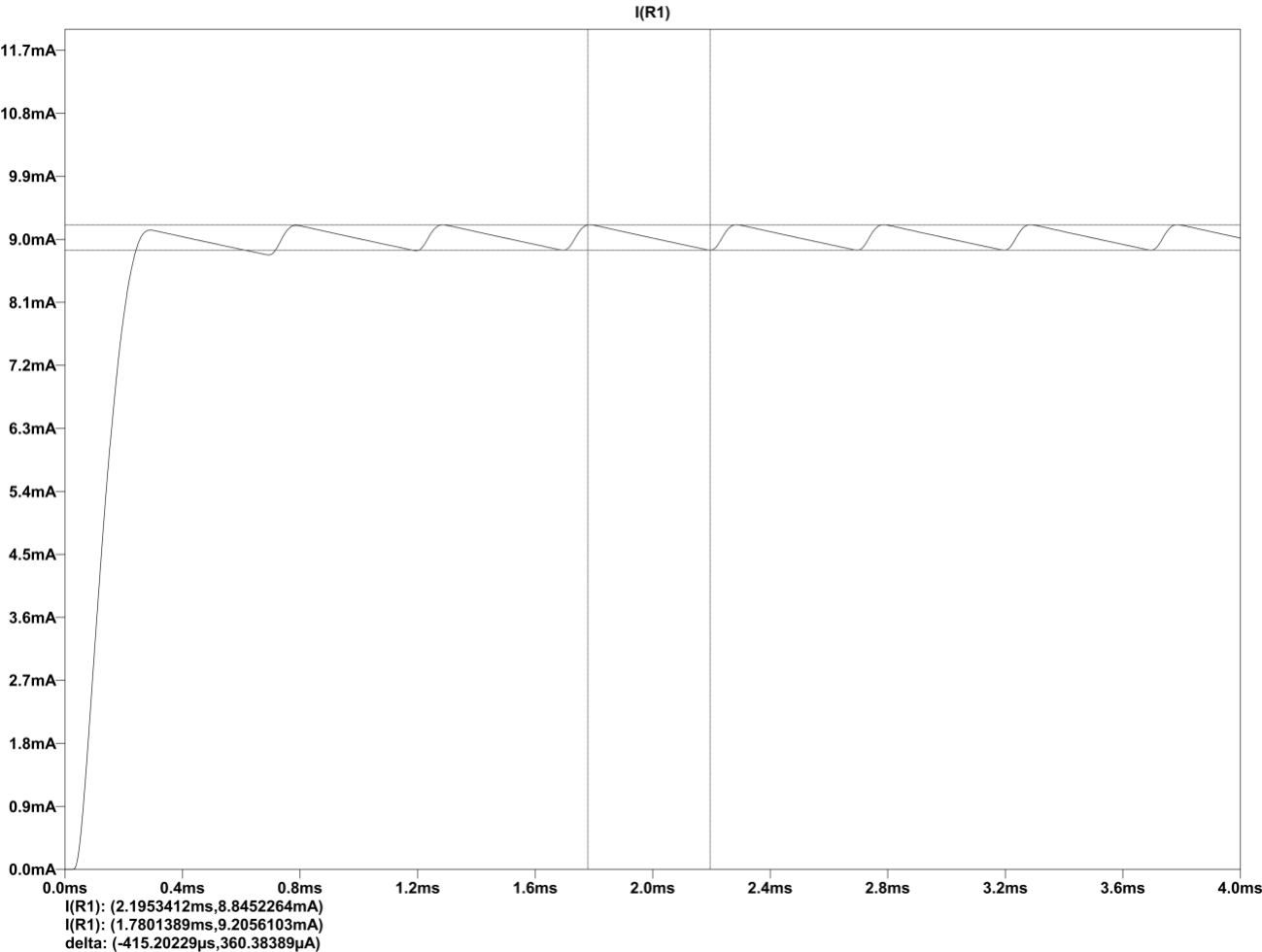
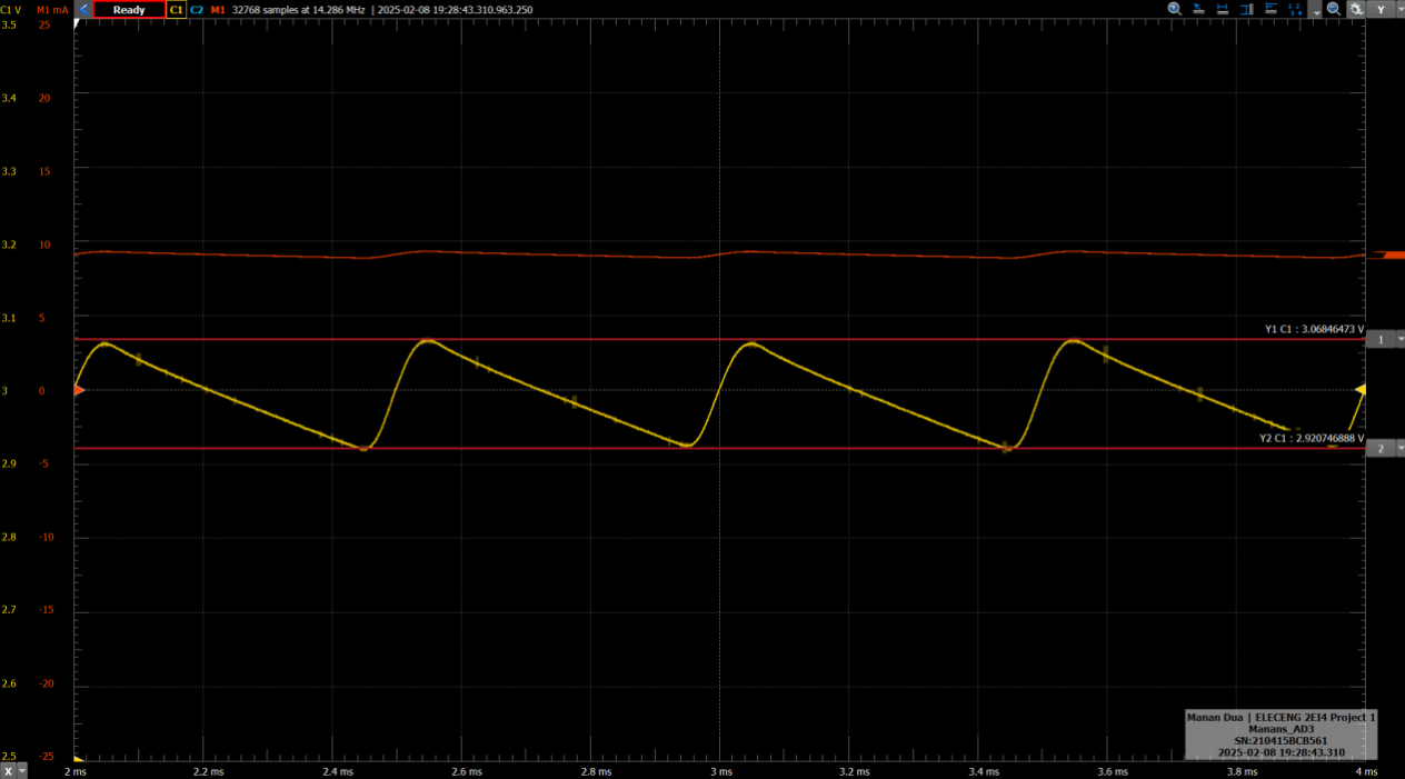
An AC-to-DC converter transforms alternating current (AC) from a source into direct current (DC), required by most electronic devices. This project’s objective was to design and build a DC power supply capable of delivering 10 mA at 3 V ± 0.1 V from a 120 V (rms), 1 kHz source. Core stages include a transformer (or direct AD3 source), a center-tapped full-wave rectifier, a filter capacitor, and a load resistor.

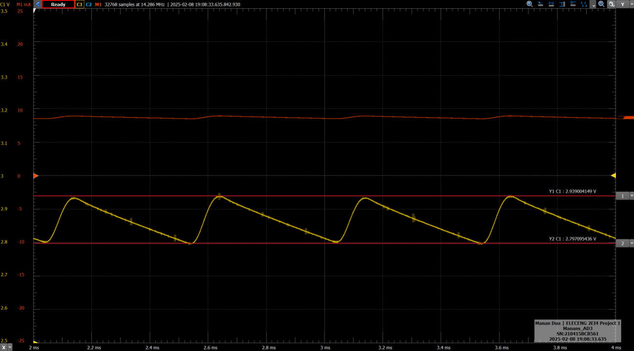
The major design requirement: output 3 V ± 0.1 V at 10 mA. Secondary requirements include maintaining ripple under 0.2 V p-p and ensuring component availability (e.g., 330 Ω resistor vs. ideal 300 Ω).

Components of an AC-to-DC Converter (Figure 1)

Design

Circuit Topology

A center-tapped full-wave rectifier was chosen over half-wave or bridge topologies to reduce ripple and utilize both halves of the AC cycle.

The initial circuit model (Figure 2) guided part value calculations. No regulator was omitted since the filter maintains output within tolerance; however, it could improve stability if added.

Initial circuit model (Figure 2)

Component Details

The key components selected for this design include:

  • Load Resistor (RL): Defines output current at 10 mA for 3 V.
  • Filter Capacitor (Cf): Smooths output to maintain ±0.1 V ripple.
  • Rectifier Diodes (D₁, D₂): Two 1N4148 diodes for center-tapped rectification.
  • Transformer: Center-tapped, step-down from 120 V (rms) to required Vpeak. (Not physically used; AD3 waveform generator substituted.)

Calculations

Load Resistor (RL)

Given Vout = 3 V ± 0.1 V and Iout = 10 mA:

V_out = I_out × R_L
R_L = 3 V / 10 mA = 300 Ω
P_L = 3 V × 10 mA = 0.03 W

Nearest available resistor: 330 Ω (0.25 W rating) was chosen—within acceptable tolerance.

Filter Capacitor (Cf)

Desired ripple: Vpp ≤ 0.2 V; output frequency fripple = 2000 Hz.

C = I_out / (V_pp × f_ripple)
  = 10 mA / (0.2 V × 2000 Hz) 
  = 25 µF

Available capacitors: three 10 µF units in parallel = 30 µF total.

Rectifier & Diode Drop

Center-tapped full-wave rectifier with 1N4148 diodes (drop ≈ 0.72 V).

V_peak = V_C + V_D 
       = 3.1 V + 0.72 V ≈ 3.82 V

Thus, each secondary half-cycle sinusoid must reach ±3.82 V peak.

Transformer Turns Ratio

If a center-tapped transformer were used with 120 Vrms input:

  • Desired secondary RMS: ~5.40 V_rms.
  • Turns ratio Nprimary / Nsecondary ≈ 22:1.

Circuit Schematic

The completed schematic, with calculated component values inserted, is shown below. Note: transformer omitted; AD3 waveform generator substituted at the center-tap inputs.

Circuit schematic with specific component values (Figure 5)

Measurement & Analysis

Physical Build

The circuit was assembled on a breadboard using:

  • AD3 waveform generator outputs (two center-tapped signals, 3.82 V_pp, 180° out of phase).
  • Two 1N4148 diodes in center-tapped configuration.
  • Filter: 30 µF total.
  • Load resistor: 330 Ω.
Physical circuit using components

Initial Waveform Settings

AD3 set to produce two sine waves, 3.82 Vpp each, 180° apart—intended to yield ~3 V DC after rectification and filtering.

Initial waveform generator settings

Initial Output Observation

Measured DC output: ~2.80 V–2.94 V ripple (below desired 2.9 V–3.1 V range). Resulting output current: 8.7 mA–9.3 mA (expected due to 330 Ω vs. 300 Ω).

Initial circuit output with cursors

Adjusted Waveform Settings

Increased AD3 amplitude to 3.95 V_pp per half-cycle to compensate for higher diode drop (~0.9 V measured) and resistor tolerance.

Modified waveform generator settings

Corrected Output Observation

Measured DC output: ~2.92 V–3.07 V ripple, within specification. Output current: ~8.7 mA–9.3 mA, consistent with resistor choice.

Output with modified input values

Simulation

LTSpice Simulation Setup

A transient simulation (0 ms–4 ms) was run in LTSpice, using:

  • Two voltage sources: V1 N002 0 SINE(0 –3.82 1000) and V2 N001 0 SINE(0 3.82 1000).
  • Diodes: 1N4148 (LTSpice default model).
  • Filter capacitor: 30 µF.
  • Load resistor: 330 Ω.
Simulation schematic

Voltage Simulation Results

Output voltage waveform: peak ~3.03 V, ripple ~0.1 V (within spec). Voltage peaks occur when one diode is forward-biased; during valleys, both diodes are off and capacitor discharges.

Voltage output from simulation

Current Simulation Results

Output current waveform: ~8.8 mA–9.2 mA. Current ripple reflects voltage ripple through the 330 Ω load.

Current output from simulation

Discussion

Comparing calculations, simulation, and measurements reveals discrepancies due to component tolerances and diode forward voltage variations. Simulation closely matched calculations (peak ~3.03 V vs. 3.1 V). Physical measurements required raising input to 3.95 V_pp to compensate for actual diode drop (~0.9 V vs. assumed 0.72 V) and resistor tolerance.

Output current ripples (8.7 mA–9.3 mA measured, 8.8 mA–9.2 mA simulated) aligned closely, given 330 Ω load. RC filter choice proved adequate, though an LC filter would reduce losses but increase complexity and cost.

Limitations:

  • AD3 waveform generator max ±5 V (800 mA); limits maximum load to ~4 W with this rectifier topology.
  • Tolerance stack-up: diode forward voltage ±5%, resistor ±5%, capacitor ±10%—combined tolerance impacts output voltage accuracy.
  • RC filter: dissipates ripple energy in resistor; LC filter would be more efficient but bulkier and costlier.
  • No dedicated voltage regulator: stability relies on filter and input adjustment.

Overall, the DC power supply met specifications after adjusting input amplitude. Ensuring accurate component values (e.g., measuring diode drops) and tight tolerances would further improve performance.

References

  1. A. S. Sedra, K. C. Smith, T. C. Carusone, and V. Gaudet, Microelectronic Circuits, 8th ed. New York, NY: Oxford University Press, 2019.
  2. “Components—Part 1: The Capacitor is the Simplest Noise Filter,” Learn about Technology with TDK, 2024. Link.
  3. Electrical Technology, “What is a Rectifier? Types of Rectifiers and their Operation,” Electrical Technology, Jan 15, 2019. Link.
  4. J. Colvin, “Analog Discovery 3 Reference Manual,” Digilent, 2023. Link.
  5. “1N4148 / 1N4448” Datasheet, Diodes Inc., 2008. Link.