FPGA Image Decompressor on Altera DE2-115
Verilog / SystemVerilog Altera DE2-115 FPGA ModelSim Quartus Prime Python

Overview & Purpose

This project, developed for the COE 3DQ5 (Digital Systems Design) course, involved designing and implementing a hardware-accelerated image decompression system on an Altera DE2-115 FPGA. The primary goal was to receive a compressed image in the custom .mic19 bitstream format via UART, decode it in real-time using custom hardware logic, and display the resulting decompressed image on a monitor via a VGA interface.

Modern image processing often requires specialized hardware to handle high-throughput data streams efficiently. By offloading complex tasks such as Inverse Discrete Cosine Transforms (IDCT) and Color Space Conversion from a general-purpose processor to the FPGA, we demonstrated the power of parallelism in digital system design. The project required rigorous timing analysis, resource optimization, and the implementation of a robust finite state machine (FSM) to manage data flow between the UART, SRAM, and the display pipeline.

Team & Collaboration

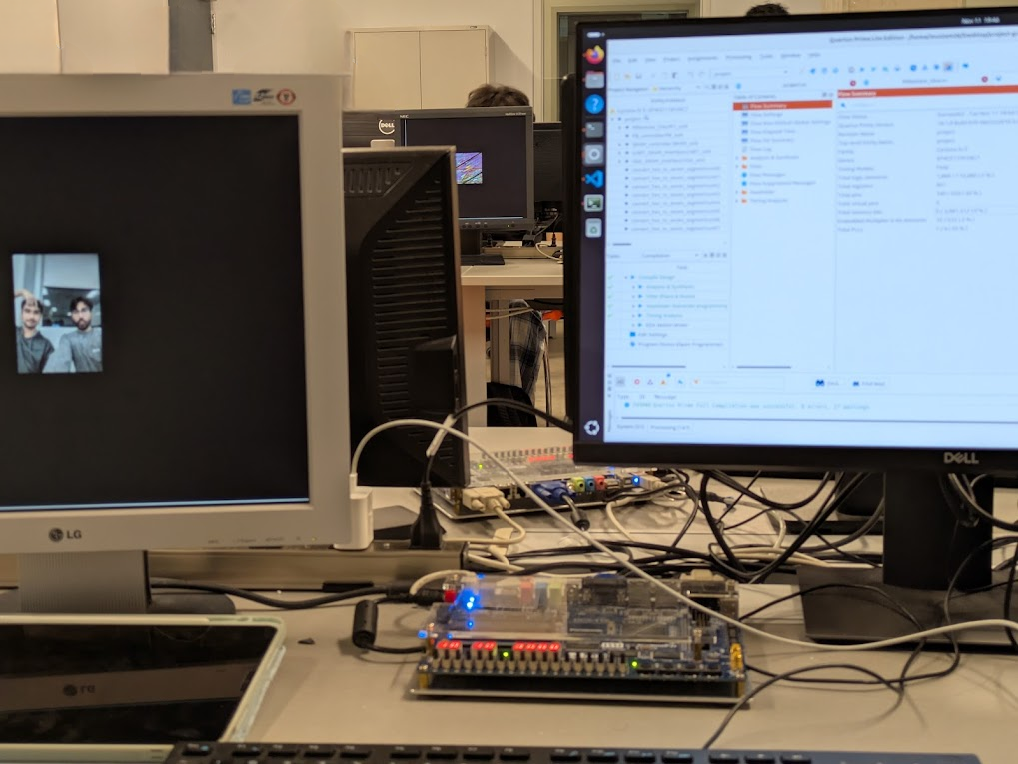
This project was a deep collaborative effort between myself (Manan Dua) and my partner, Mohammad Mustafa. Unlike typical projects where components are split entirely, we worked together on the conceptualization, state machine design, and board testing for every single milestone. We utilized pair programming for the critical debugging phases to solve complex timing violations.

To maximize efficiency, we divided the specific implementation tasks within each milestone:

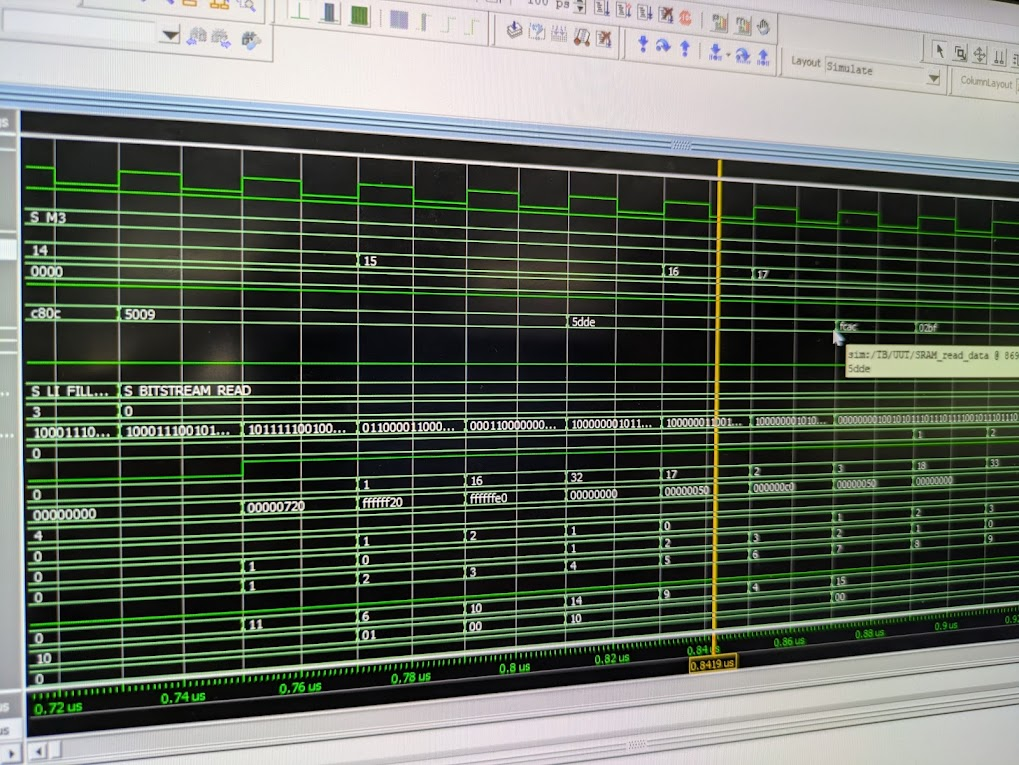
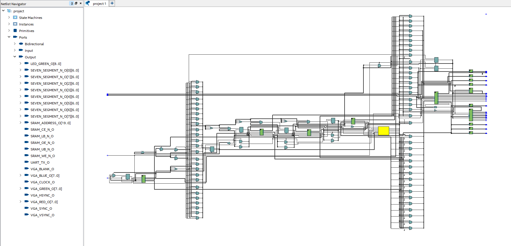
  • Manan Dua: Took the lead on the second pass of the IDCT (Compute S) and adapting the arithmetic logic for the Chroma planes during Milestone 2. For Milestone 3, I designed the "Zig-Zag" address counters and the Quantization logic required to reconstruct frequency coefficients from the bitstream.
  • Mohammad Mustafa: Optimized register usage in Milestone 1 to ensure we met resource constraints. In Milestone 2, he led the implementation of the first IDCT pass (Compute T). For Milestone 3, he focused on the "Burst Write" logic for the SRAM interface to ensure the decoded data was written back to memory efficiently.
FPGA Lab Setup

Components & Architecture

The system is built on the Altera DE2-115 Development Board, operating at a clock frequency of 50 MHz. The data flow architecture consists of:

  • Communication Interface: A UART receiver operating at 115200 baud to fetch the compressed .mic19 bitstream from a PC.
  • Memory Management: An SRAM Controller that manages the 2MB off-chip SRAM. It handles the critical task of arbitration, allowing the system to simultaneously write incoming compressed data and read out decompressed pixel data for the display.
  • VGA Controller: Generates the necessary H-Sync and V-Sync signals to drive a standard monitor at 640x480 resolution.
Waveform Diagram

Build Process & Milestones

Milestone 1: Colour Space Conversion & Upsampling

The Task: In image compression, color data (Chroma, or U/V) is often downsampled (stored at lower resolution) to save space because the human eye is less sensitive to color detail than brightness (Luma, or Y). Our task was to restore the full resolution image. This involved implementing a 10-tap interpolation filter to "guess" the missing color pixels (Upsampling) and then performing matrix multiplication to convert the YCbCr data into the standard RGB format for the monitor.

The Constraint: Hardware multipliers (DSP blocks) are a limited resource on an FPGA. We were restricted to using only 4 hardware multipliers for this entire stage. To prove our design was efficient, we were required to achieve a utilization rate of at least 80%.

Our Implementation: We designed a state machine that reused partial products in the matrix multiplication to minimize calculations.

  • Result: We achieved a multiplier utilization rate of 83.33% (using 30 out of 36 available multiplication slots in our pipeline).
  • Throughput: The processing of one pixel row (which involves calculating 320 pixels) took approximately 864 clock cycles.
  • Resource Usage: This complex module consumed 550 registers on the FPGA.

Milestone 2: Inverse DCT (IDCT)

The Task: JPEG compression stores images as frequencies (waves) rather than pixels. To display the image, we must convert these frequency coefficients back into spatial pixel data. This requires an Inverse Discrete Cosine Transform (IDCT), a computationally heavy operation involving transforming 8x8 and 16x16 matrices.

The Constraint: Storing these large matrices consumes significant on-chip memory. We were allowed to use up to 4 Dual-Port RAMs (DPRAMs) to buffer the data. We were also restricted to using only 3 hardware multipliers for the IDCT math, with a target utilization of >85%.

Our Implementation: We decomposed the 2-D IDCT into two 1-D passes (processing rows first, then columns). We utilized the 4 DPRAMs to store intermediate results (S' and T matrices) and the Transpose matrix (C), optimizing the read/write patterns to keep the pipeline full.

  • Result: We achieved extremely high efficiency, with multiplier utilization rates of 88% for Luma blocks and 87% for Chroma blocks.
  • Resource Usage: This complex module consumed only 357 registers on the FPGA.

Milestone 3: Lossless Decoding & Quantization

The Task: This was the final piece of the puzzle: reading the raw compressed bitstream (.mic19 format) from memory. Compressed data is variable-length (a simple "white" block might take 2 bits, while a complex texture might take 100 bits). We had to parse this stream, identify the codes, and perform Requantization to reconstruct the frequency coefficients for the IDCT stage.

The Constraint: Since multipliers are scarce and were largely used in previous stages, we were required to use variable shifters (bit-shifting logic) instead of multipliers for the Requantization step.

Our Implementation: We implemented "zig-zag" scanning logic to correctly place the decoded coefficients into the 8x8 and 16x16 matrices.

  • Engineering Analysis: We calculated the worst-case latency for a Luma block to be 864 clock cycles and a Chroma block to be 216 clock cycles.
  • Bottleneck Identification: Our analysis revealed that a seamless real-time pipeline was difficult because fetching the bitstream from SRAM pauses the arithmetic pipeline. To fully meet the integration timing, the bitstream fetching would need to be decoupled and run as a background process to hide this latency. Unfortunately, due to time contraints, we were not able to complete milstone 3 to the fullest extent which would be merging the requantized values with the Compute T stage of milestone 2. However the core functionality was implemented independently of milestone 2 successfully.
  • Resource Usage: This complex module consumed only 197 registers on the FPGA.

RTL Schematic View

Results

The final design successfully met the core project specifications, correctly decoding and displaying the test images.

  • Total Resources: The entire project utilized 4,586 Logic Elements on the FPGA.
  • Functionality: The system reliably decompressed the .mic19 format and displayed it on the monitor with no visual artifacts.
  • Design Quality: We achieved a fully synchronous design without any latches, ensuring robustness against timing glitches and reliable operation on the FPGA hardware.
Final Decompressed Image on VGA

Reflections & Learnings

This project was a deep dive into the complexities of digital system design. We learned significant lessons about:

  • Matrix Operations in Hardware: How to efficiently perform matrix multiplication on data stored in RAM and manage the storage of intermediate results.
  • Variable Latency: Handling circuits and modules that take variable amounts of time to complete tasks, and designing interfaces that can wait or stall correctly without losing data.
  • Project Management: The importance of breaking a complex system into smaller, testable modules and effectively assigning concurrent tasks to maximize team efficiency.