Physical Build of Voltage Switch
CD4007 MOSFET Array LTSpice Simulation Transmission Gates Analog Circuit Design Breadboarding

Introduction

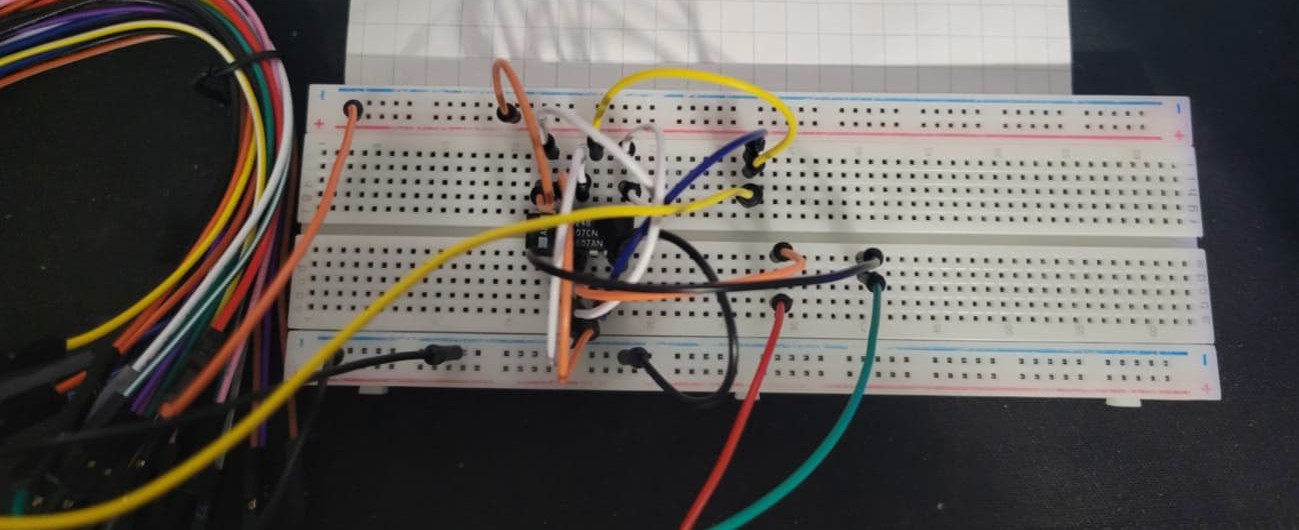
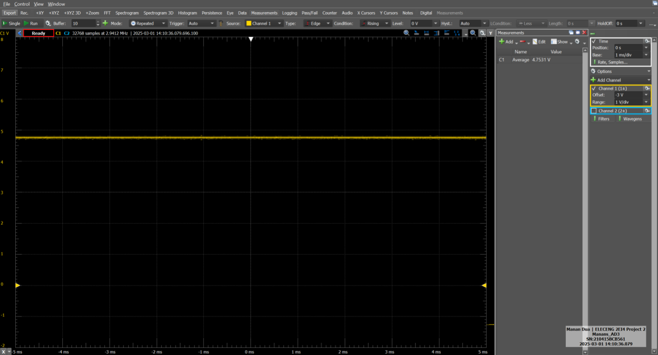
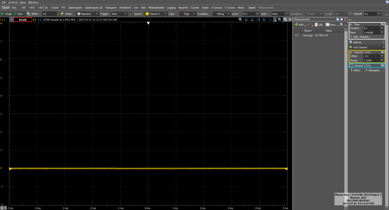
In this project, two voltage-controlled switches were designed, built, and tested using CD4007 MOSFET arrays. Each switch’s performance was evaluated against the ideal-switch model by examining four non-idealities: on-state resistance (Ron), off-state leakage (Roff), limited voltage range, and bidirectional capability. Measurements were compared to LTSpice simulations to understand practical deviations.

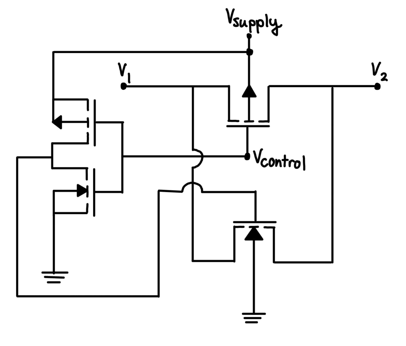
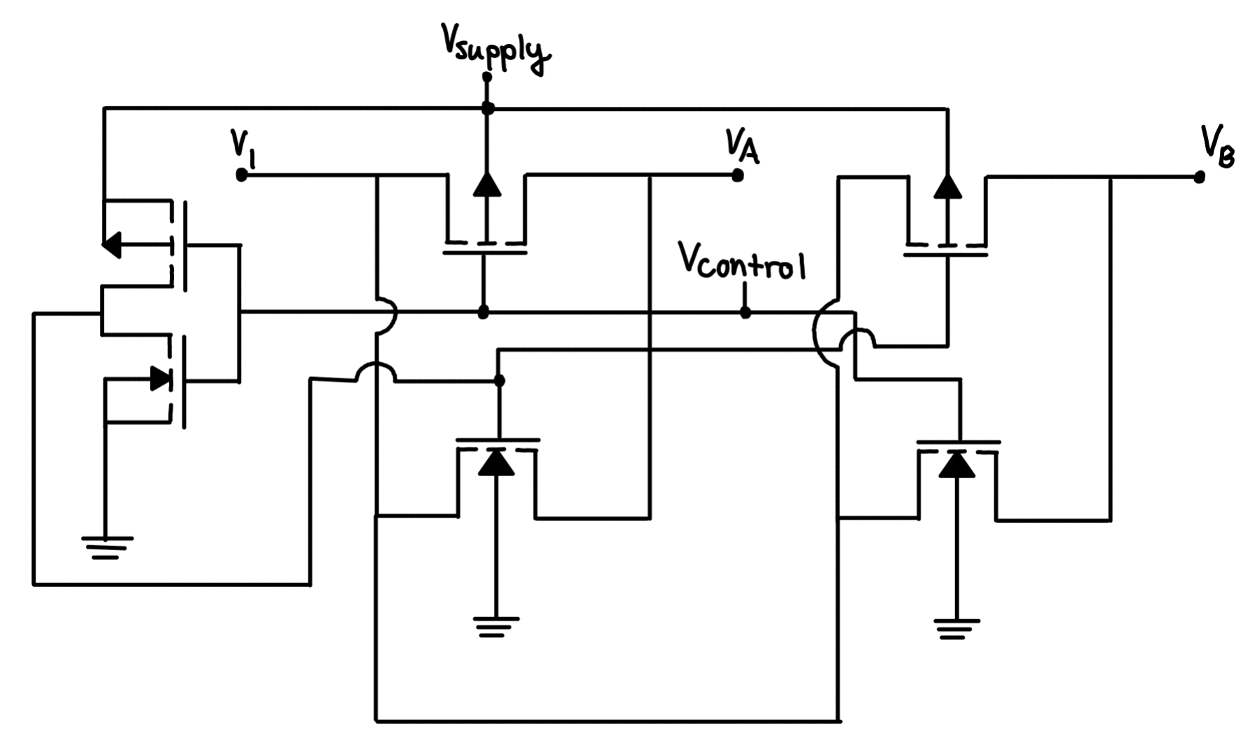
Switch Type 1: Single transmission gate formed by an NMOS and PMOS in parallel, controlled by Vcontrol and its inverse.
Switch Type 2: Two transmission gates arranged to select between two outputs (VA or VB), behaving like a 2:1 multiplexer.

Ideal vs. Non-Ideal Switches

Ideal Switch Properties

  • Zero on-state resistance (Ron = 0), producing no voltage drop or power loss.
  • Infinite off-state resistance (Roff → ∞), ensuring zero leakage current when open.
  • Ability to handle any voltage difference without breakdown.
  • Constant Ron, independent of applied voltage.

Non-Idealities (Real)

  • Non-zero Ron: Measurable voltage drop and power dissipation in ON state.
  • Finite Roff: Leakage current flows when switch is OFF.
  • Limited Voltage Range: Switch only operates within a certain Vin range.
  • Directional Dependence: Ron may differ depending on current direction.

Test Plan

Each switch was tested under these four conditions using a 10 kΩ pull-down resistor.

1. On-State Resistance

Apply V1=5 V, Vcontrol=0 V. Measure Vout and calculate Ron via voltage divider law.

2. Off-State Leakage

Apply V1=5 V, Vcontrol=5 V. Measure Vout to compute leakage current and Roff.

3. Operating Voltage

Apply a 5 Vpp sinusoid at 10 Hz to V1. Observe Vout vs. Vin to find threshold anomalies.

4. Bidirectional

Swap input to previously output node with Vcontrol=0 V. Measure Vother to compute reverse Ron.

Switch Type 1: Single Transmission Gate

Switch 1 LTSpice Schematic (Figure 5)

Circuit Description

Switch 1 is a single transmission gate implemented on a CD4007. An NMOS and PMOS are arranged in parallel, with gates driven by Vcontrol and its inverted signal (generated via two additional MOSFETs). This ensures conduction for any input between 0 V and 5 V.

On-State Resistance (Ron)

Test Conditions: Vsupply=5 V, V1=5 V, Vcontrol=0 V, 10 kΩ pull-down at V2. Measured V2≈4.75 V.

R_on = [V1 × 10kΩ / V2] – 10kΩ 
     = [5V × 10kΩ / 4.75V] – 10kΩ 
     ≈ 526 Ω
          
V2 Measurement for Ron
V2 Measurement for Leakage

Off-State Leakage

Test Conditions: Vsupply=5 V, V1=5 V, Vcontrol=5 V, 10 kΩ pull-down at V2. Measured V2≈19.2 mV.

Calculated Leakage Ileak ≈ 1.92 µA.
Effective Roff ≈ 2.59 MΩ.

Operating Voltage Range

Test Conditions: Vsupply=5 V, V1=5 Vpp sinusoid at 10 Hz (±2.5 V), offset 2.5 V, Vcontrol=0 V. Measured V2 follows V1 for most of the 0–5 V range, but shows a slight deviation at ~2.4 V due to MOSFET threshold mismatches during the transition between NMOS and PMOS dominance.

V2 vs V1 Voltage Range
Transmission Gate Operation

Theoretical Analysis & Trade-offs

Switch 1 is a classic CMOS transmission gate. The parallel NMOS/PMOS configuration ensures that for any Vin (0–5 V), at least one device conducts. However, it requires 4 MOSFETs (leaving 2 unused on the CD4007), and the measured Ron (~500 Ω) is higher than ideal due to the specific device parameters and the 10 kΩ load.

Switch Type 2: 2:1 Multiplexer

Circuit Description

Switch 2 extends Switch 1 by adding a second transmission gate (TG2) controlled by the inverted Vcontrol. TG1 connects V1 to VA when Vcontrol=0 V; TG2 connects V1 to VB when Vcontrol=5 V. Thus, only one of VA or VB is connected at a time.

Switch 2 LTSpice Schematic
Switch 2 Physical Build

Physical Build

Built on a breadboard using two CD4007 ICs (one per transmission gate), plus two inverters for complementary control. 10 kΩ pull-down resistors are placed on VA and VB.

Performance Measurements

  • Ron: Measured ~504 Ω for both channels (VA and VB).
  • Leakage: Off-state leakage measured ~4.5 µA, resulting in an Roff of ~1.1 MΩ.
  • Bidirectional: Confirmed reverse conduction with Ron,reverse ≈ 504 Ω.

Functionally, this switch resembles a multiplexer. The trade-off is higher component cost (two ICs) and increased complexity compared to the single transmission gate.

Switch 2 Voltage Range

References

  1. “CD4007UB Types,” Texas Instruments, Datasheet.
  2. W. Storr, “Transmission gate as a CMOS bilateral switch,” Basic Electronics Tutorials, Article.
  3. A. S. Sedra, K. C. Smith, T. C. Carusone, and V. Gaudet, Microelectronic Circuits, 8th ed. New York, NY: Oxford University Press, 2019.